Imec Bridges the Gap Between Quantum Physics and Industrial Fabrication With High-NA EUV
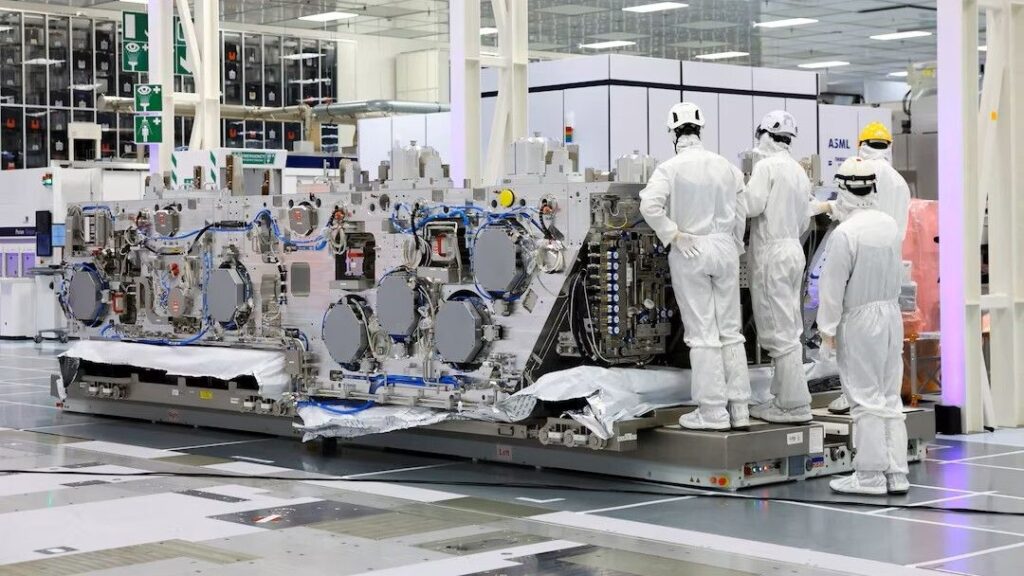
Table of Contents
Moving Beyond the Lab
For years, the primary tension in quantum computing hasn’t been whether the physics works, but whether the hardware can actually be built at scale. While companies like IBM and Google have demonstrated impressive qubit counts using superconducting loops, the industry has long struggled with the ‘ reproducibility crisis’—the difficulty of manufacturing millions of identical, controllable qubits across a silicon wafer without catastrophic variance.
Imec, the Belgian semiconductor research hub, may have just shifted that trajectory. At the ITF World event in Leuven, the organization unveiled the first quantum dot qubit device fabricated using High-NA EUV (High Numerical Aperture Extreme Ultraviolet) lithography. By applying the industry’s most advanced chip-making tool to quantum hardware, Imec is attempting to move quantum computing out of the realm of artisanal laboratory assembly and into the world of industrial semiconductor fabrication.
The Precision Problem
The device utilizes silicon quantum dot spin qubits, which function by trapping individual electrons in nanoscale structures. These electrons store information via their quantum spin states, while surrounding metallic control gates manipulate their interactions. The efficacy of these qubits depends entirely on the precision of the spacing between these electrodes; as the gaps shrink, the coupling strength and interaction fidelity improve exponentially.
Until now, achieving the necessary tolerances has been a bottleneck. Imec has successfully patterned these devices with gate gaps of just 6 nanometers. To put that in perspective, a human hair is roughly 80,000 to 100,000 nanometers wide. Achieving this level of consistency across a 300mm wafer is less of a physics challenge and more of a brutal engineering one.
Leveraging the ASML Powerhouse
The breakthrough was made possible by the deployment of High-NA EUV technology, the latest evolution in lithography developed by ASML. While standard EUV systems have a numerical aperture of 0.33, the High-NA systems push this to 0.55. This isn’t a simple incremental update; it requires an entirely redesigned optical system with mirrors polished by Zeiss to atomic precision and a machine footprint that spans the length of a double-decker bus.
High-NA EUV is currently the ‘holy grail’ for the traditional semiconductor industry, intended for the production of sub-2nm processors and next-generation AI accelerators. Intel only recently installed its first commercial tool, and Imec integrated the technology into its cleanroom in March 2026. By utilizing this machinery for quantum dots, Imec is essentially piggybacking on the multibillion-dollar infrastructure of the CMOS industry.
Industrializing the Qubit
The strategic implication here is clear: if quantum hardware can be built using the same tools as a Snapdragon or an Apple M-series chip, the timeline for fault-tolerant quantum computing could compress significantly. This approach bypasses the need for a separate, exotic fabrication ecosystem, allowing quantum developers to leverage decades of existing transistor scaling expertise.
However, the road to a commercially viable machine remains long. While 6nm gaps are a triumph of fabrication, the industry still faces the massive challenge of error correction and maintaining coherence across millions of qubits. Most industry roadmaps, including those from Quantinuum and PsiQuantum, don’t expect fully fault-tolerant systems until 2030 or beyond.
Still, by proving that High-NA EUV can reliably produce the architecture required for spin qubits, Imec has removed one of the most daunting hurdles in the path to scale. The question is no longer just if we can make a qubit, but whether we can print them by the millions.