AMD SP7 and Intel Diamond Rapids Sockets Debuted: The Era of 1,400W Server CPUs
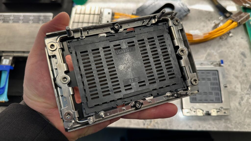
Table of Contents
The Physical manifestation of the AI Compute Boom
At Computex 2026, the sheer physical scale of the next generation of data center compute became apparent. While most consumers focus on software like LLMs and generative AI, the underlying hardware is undergoing a massive architectural shift to support the power and bandwidth these models demand. The unveiling of AMD’s SP7 socket and Intel’s gargantuan 9,324-pin socket marks a departure from incremental updates, signaling a move toward monolithic power delivery and unprecedented I/O density.
- AMD SP7 will support 6th Gen EPYC “Venice” processors with up to 256 cores and potential 1,400W peak power draws.
- Intel’s Diamond Rapids platform utilizes a massive 9,324-pin socket, targeting 192 cores and PCIe 6.0.
- Thermal Shift: Both platforms are pushing peak power consumption beyond 1kW, making liquid cooling a requirement rather than an option.
- Memory Evolution: The move toward MRDIMMs and 16-channel configurations is designed to eliminate the “memory wall” in AI training.
AMD SP7: Powering EPYC Venice and the 512-Core Server
The AMD SP7 socket is the foundation for the upcoming 6th Generation EPYC “Venice” processors. In a live demonstration at Computex, the socket’s dimensions were striking, occupying nearly the entire palm of a human hand. This isn’t merely for aesthetic reasons; the increase in surface area is a direct result of the pin density required for modern high-performance computing (HPC).
According to early technical data from cooling partner Auras, the SP7 is designed to handle CPUs with a peak power consumption reaching 1,400W. To put this in perspective, a standard high-end consumer CPU typically peaks around 250W-300W. We are seeing a shift where a single processor socket now consumes as much power as several high-end gaming PCs combined.
The Technical Specs of Venice
AMD is leveraging the SP7 to push the boundaries of core counts. With EPYC Venice, AMD aims for up to 256 cores per socket. In a dual-socket configuration, this allows system integrators to build servers boasting 512 x86 cores in a single chassis. This density is critical for virtualization and massive parallel workloads.
Beyond cores, the I/O throughput is the real story. The SP7 is rumored to support 16 DDR6 memory channels utilizing 12.8 GT/s MRDIMMs (Multi-Rank Dual In-line Memory Modules). Furthermore, the platform integrates up to 96 PCIe 6.0 lanes, providing the massive bandwidth necessary for CXL (Compute Express Link) protocols, which allow the CPU to share memory with GPUs and accelerators more efficiently.
Intel’s Diamond Rapids: The 9,324-Pin Behemoth
While AMD is moving faster with a 2026 rollout, Intel is preparing a platform that is physically larger than anything seen in the x86 ecosystem. The socket for Xeon Diamond Rapids features a staggering 9,324 pins. This massive pin count is likely intended to ensure signal integrity for the higher clock speeds and increased voltage required by the next generation of Xeon processors.
Diamond Rapids is expected to launch in 2027, featuring up to 192 cores. While the core count is lower than AMD’s Venice, Intel’s strategy focuses on the efficiency of those cores and the robustness of the interconnects. Like AMD, Intel is moving toward a 16-channel DDR5 memory subsystem supporting MRDIMMs and full PCIe Gen6 support.
Power and Thermal Challenges
Intel has not yet officially disclosed the Processor Base Power (PBP) for Diamond Rapids. However, the fact that Auras is already developing dedicated water blocks for this socket suggests that peak power will easily exceed 1kW. Industry analysts estimate a PBP between 300W and 500W, with transient spikes pushing well into the four-digit wattage range.
Interestingly, the sheer size of the 9,324-pin socket suggests Intel may be designing for longevity. It is highly probable that this same socket will be utilized for the subsequent Coral Rapids processors, expected around 2028 or 2029, to avoid forcing data center operators to replace motherboards every 12 months.
| Feature | AMD SP7 (Venice) | Intel 9324-Pin (Diamond Rapids) |
|---|---|---|
| Expected Launch | 2026 | 2027 |
| Max Core Count | Up to 256 Cores | Up to 192 Cores |
| Peak Power Draw | ~1,400W | 1,000W+ |
| Memory Support | 16-Channel DDR6 / MRDIMM | 16-Channel DDR5 / MRDIMM |
| Interconnect | PCIe 6.0 / CXL | PCIe 6.0 |
What This Means for the Data Center
The transition to these massive sockets represents more than just “bigger chips.” It is a fundamental shift in how servers are built. For the average IT manager, this implies three critical changes:
1. The End of Air Cooling: When a single CPU can draw 1,400W, traditional heat sinks and fans are no longer viable. We are entering an era where direct-to-chip liquid cooling (DLC) is the baseline requirement. This forces a massive capital expenditure upgrade for data center infrastructure to support coolant loops.
2. The Memory Wall Breakdown: By implementing 16 memory channels and MRDIMMs, AMD and Intel are addressing the bottleneck where CPUs spend more time waiting for data from RAM than actually processing it. This is essential for AI workloads where the datasets are too large for on-chip cache.
3. Massive Parallelism: The ability to put 512 cores in a dual-socket server means that monolithic applications that can scale across thousands of threads will see unprecedented performance gains, potentially reducing the number of physical servers needed to run a specific workload.
The Mid-Range Alternative: AMD SP8
Recognizing that not every company needs a 1,400W, 256-core monster, AMD is also preparing the SP8 platform. This socket is designed for a different tier of the market—those requiring fewer cores and a smaller number of DDR5 channels. However, the SP8 is not “low power” by consumer standards; Auras is also developing water blocks for this platform, suggesting that even the mid-range server market is shifting toward liquid cooling.
Technical Definition: What is an MRDIMM?
MRDIMM (Multi-Rank Dual In-line Memory Module) is a high-performance memory architecture that integrates a buffer on the module to allow higher data rates. By reducing the electrical load on the memory controller, MRDIMMs enable the CPU to push more data at higher frequencies (such as 12.8 GT/s) without compromising stability, effectively increasing the total memory bandwidth available to the processor.
FAQ: Understanding Next-Gen Server Hardware
Will these sockets be compatible with existing motherboards?
No. Both the AMD SP7 and Intel’s 9,324-pin sockets are entirely new physical interfaces. Upgrading to EPYC Venice or Xeon Diamond Rapids will require new motherboards and likely new power delivery systems to handle the increased wattage.
Why does the pin count matter so much for Intel?
More pins allow for more dedicated power rails and more data lanes. As CPUs increase in core count and speed, they require more precise voltage regulation and more “paths” for data to travel between the CPU and the RAM/PCIe devices to avoid bottlenecks.
Is PCIe 6.0 actually necessary for server CPUs?
Yes, especially for AI. PCIe 6.0 doubles the bandwidth of PCIe 5.0. When you have hundreds of cores requesting data from NVMe drives or GPU accelerators, the bus can become a bottleneck. PCIe 6.0 ensures the data pipe is wide enough to keep the cores fed.
How do you cool a 1,400W CPU?
Standard air cooling cannot move heat fast enough for a 1.4kW load. These systems use cold plates—copper blocks that sit directly on the CPU—with liquid coolant circulating to a heat exchanger or a facility-wide cooling loop.
What is the difference between AMD SP7 and SP8?
The SP7 is the high-end flagship socket for the most powerful EPYC Venice chips. The SP8 is a targeted platform for lower core counts and DDR5 memory, aimed at a slightly more modest (though still powerful) server market.