Huawei Proposes ‘Tau Scaling Law’ as Moore’s Law Hits Physical Limits
Table of Contents
The Wall of Physical Limits
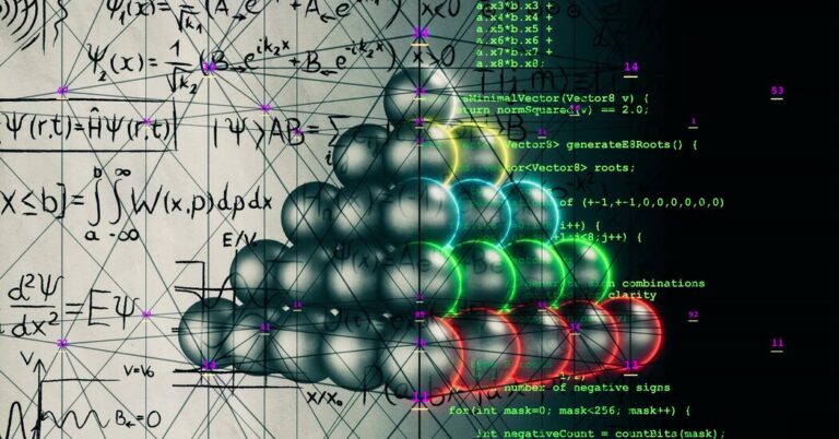
For nearly six decades, the semiconductor industry has operated under a predictable, almost religious, cadence: the doubling of transistors on a microchip roughly every two years. This empirical observation, formulated by Intel co-founder Gordon Moore in 1965, has driven everything from the first mainframe computers to the modern smartphone. But as the industry pushes toward the 2nm threshold, the math is starting to break.
The current race—headlined by TSMC, Samsung, and Intel—is no longer just about engineering precision; it is a fight against the laws of physics. At the 2nm scale, quantum tunneling (where electrons leak across barriers they should not be able to cross) and extreme heat density make traditional scaling nearly impossible. Samsung has already moved toward mass production for its next-generation Exynos chipsets, and TSMC is refining its Gate-All-Around (GAA) transistor architecture to maintain efficiency. Yet, these are incremental victories in a game that is fundamentally reaching its end.
Enter Huawei. The Chinese tech giant, which has spent years navigating stringent US sanctions on high-end chip equipment, is now arguing that the industry needs to stop trying to save Moore’s Law and instead replace it entirely. Their proposed alternative is the Tau Scaling Law.
Beyond Transistor Density
While Huawei has not released a complete technical white paper detailing every mechanism of Tau Scaling, the conceptual shift is clear: the focus is moving away from mere density (how many transistors you can cram into a square millimeter) toward system-level efficiency and heterogeneous integration.
The Tau Scaling Law suggests that computational gains will no longer come from shrinking the individual transistor, but from optimizing the interplay between different types of computing cores, advanced 3D packaging, and the integration of photonic interconnects. Essentially, if you can’t make the components smaller, you make the communication between them faster and the arrangement more three-dimensional.
This shift mirrors a broader trend in the industry. We are seeing this in the rise of chiplets—where different parts of a processor are manufactured on different nodes and stitched together—and in the move toward specialized AI accelerators that prioritize data throughput over raw clock speed. By pivoting to a scaling law that accounts for power efficiency and interconnect latency rather than just gate count, Huawei is attempting to redefine what ‘progress’ looks like in silicon.
The Geopolitical Subtext
The timing of this proposal is not accidental. Huawei’s HiSilicon division has been largely cut off from the world’s most advanced Extreme Ultraviolet (EUV) lithography machines produced by ASML. Without access to the tools required to hit the 2nm or 1.8nm marks, Huawei cannot compete in a world governed strictly by Moore’s Law.
By promoting Tau Scaling, Huawei is effectively attempting to shift the goalposts of the semiconductor war. If the industry accepts that traditional scaling is dead, Huawei’s expertise in system-level architecture and alternative packaging becomes a competitive advantage rather than a fallback for lacking EUV machines. It is a strategic move to pivot the industry toward a metric where they can actually compete—and potentially lead.
A Fragmented Future for Silicon
The industry’s reaction to Tau Scaling remains cautious. While most architects agree that Moore’s Law is slowing—or ‘dead’ in the literal sense of transistor shrinking—the transition to a new standard is rarely seamless. For developers, the promise of Tau Scaling means that software must be written to take advantage of complex, heterogeneous hardware rather than relying on the ‘free’ performance boosts that come with every new chip generation.
Whether Tau Scaling becomes the new industry gold standard or remains a theoretical framework for Huawei’s internal development depends on how these chips perform in the real world. If Huawei can demonstrate a leap in AI processing power and energy efficiency without relying on the smallest possible nodes, they may have found a way to bypass the bottleneck that currently threatens the entire global computing trajectory.