Beyond Silicon: Imec, TSMC, and ASML Hit Critical Scaling Milestone for 2D Transistors
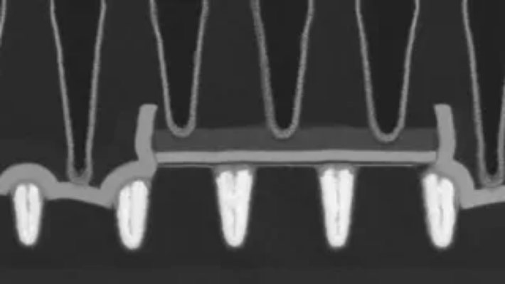
Table of Contents
The 50nm Hurdle
The semiconductor industry has long operated under the assumption that silicon would eventually hit a hard physical limit. While Gate-All-Around (GAA) architectures and nanosheets have extended the life of the silicon era, the transition to atomically thin 2D materials has remained largely confined to lab-scale demonstrations. That changed this week at the IEEE/JSAP Symposium on VLSI Technology and Circuits.
In a joint effort, imec, ASML, and TSMC revealed they have successfully integrated both n-type and p-type transistors using 2D channels on a standard 300mm wafer. The most striking detail is the 50nm contacted poly pitch—the tightest ever demonstrated for complementary 2D devices. To put that in perspective, this is tighter than the 54nm contacted gate pitch utilized in Intel’s 10nm-class nodes, effectively bringing 2D material performance into the realm of leading-edge commercial silicon.
Solving the Contact Resistance Crisis
The primary obstacle to 2D scaling hasn’t been the materials themselves, but how to connect them to the rest of the chip. Because 2D channels—such as molybdenum disulfide (MoS2) for n-channels and tungsten diselenide (WSe2) for p-channels—are atomically thin, they carry very little current. Traditional metal contacts often create a “Schottky barrier,” essentially throttling the current and forcing researchers to use oversized contact areas that defeat the purpose of scaling.
The consortium bypassed this by flipping the fabrication sequence. Rather than depositing metal onto a finished 2D film, the team implemented what imec calls a “reverse thin-film-transistor flow.” They patterned tungsten-filled contact trenches first, then transferred the 2D channel on top, finally depositing the gate over the assembly. This bottom-contact geometry resulted in a clean off-state, with both polarities stopping conduction at zero gate voltage.
According to Gouri Sankar Kar, vice president of R&D for compute and memory device technologies at imec, this approach allowed the team to achieve the 50nm CPP (contacted poly pitch) without degrading the performance of the 2D n and pFETs.
The EUV Advantage
The precision of this layout was made possible through a single-exposure EUV (Extreme Ultraviolet) step, developed in collaboration with ASML. By utilizing a single exposure to print channel lengths as short as 28nm, the team proved that standard 0.33-NA EUV scanners are sufficient for this level of integration. While ASML’s newer High-NA EUV tools are designed for even tighter pitches, this demonstration proves that the current infrastructure can handle the transition to 2D materials without requiring immediate, costly multi-patterning schemes.
The results are statistically promising: imec reported that 94% of the integrated transistors switched correctly, maintaining an on/off current ratio exceeding 100,000. This narrows the performance gap on the p-type side, which has historically been the weaker link in 2D CMOS development.
The Long Road to Production
Despite the milestone, this isn’t a product launch. The current process is “quasi-CMOS,” meaning the n- and p-type materials are transferred onto the wafer as films rather than grown in a single, monolithic process. For these to enter a fab, the industry must solve the problem of residue-free, high-throughput wafer transfer.
Timelines remain conservative. While the International Roadmap for Devices and Systems (IRDS) suggests 2D channels could appear at the 0.7nm node around 2034, imec’s own internal projections push the shift to 2D semiconductors closer to 2041. Current priorities for TSMC and Intel remain the rollout of N2 (2nm) and the eventual move to Complementary FETs (CFETs), where n- and p-type transistors are stacked vertically.
Dr. Min Cao, CTO at TSMC, noted that the collaboration is focused on “de-risking” the transition from the lab to the fab. The engineering demonstrated this week suggests that the fundamental question—whether 2D materials can actually work at scale—has been answered. The remaining hurdles are now matters of manufacturing throughput and reliability, rather than theoretical physics.